Showing posts with label Power Amplifier. Show all posts

100W MOSFET power amplifier


100W MOSFET power amplifier.

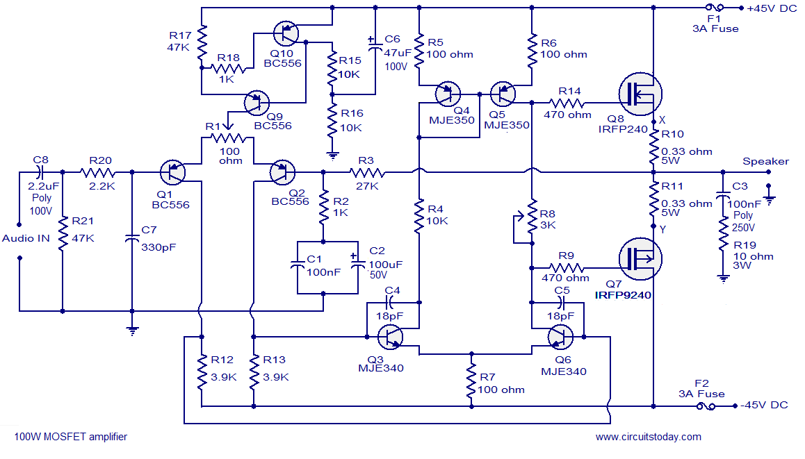
A 100W MOSFET power amplifier circuit based on IRFP240 and IRFP9240 MOSFETs is shown here. The amplifier operates from a +45/-45 V DC dual supply and can deliver 100 watt rms into an 8 ohm speaker and 160 watt rms into a 4 ohm speaker. This Hi-Fi amplifier circuit is suitable for a lot applications like general purpose amplifier, guitar amplifier, keyboard amplifier. The amplifier can be also used as a sub woofer amplifier but a subwoofer filter stage has to be added before the input stage. The amplifier has a low distortion of 0.1%, a damping factor greater than 200, input sensitivity of 1.2V and the bandwidth is from 4Hz to 4 KHz.

Circuit diagram.

mosfet power amplifier
100W mosfet power amplifier circuit

About the circuit.

Capacitor C8 is the input DC decoupling capacitor which blocks DC voltage if any from the input source. IF unblocked, this DC voltage will alter the bias setting s of the succeeding stages. Resistor R20 limits the input current to Q1 C7 bypasses any high frequency noise from the input. Transistor Q1 and Q2 forms the input differential pair and the constant current source circuit built around Q9 and Q10 sources 1mA. Preset R1 is used for adjusting the voltage at the output of the amplifier. Resistors R3 and R2 sets the gain of the amplifier. The second differential stage is formed by transistors Q3 and Q6 while transistors Q4 and Q5 forms a current mirror which makes the second differential pair to drain an identical current. This is done in order to improve linearity and gain. Power amplification stage based on Q7 and Q8 which operates in the class AB mode. Preset R8 can be used for adjusting the quiescent current of the amplifier. The network comprising of capacitor C3 and resistor R19 improves high frequency stability and prevents the chance of oscillation. F1 and F2 are safety fuses.

Circuit setup.

Set R1 at midpoint before powering up and then adjust it slowly in order to get a minimum voltage (less than 50mV0 at the output. Next step is setting up the quiescent current and keep the preset R8 in minimum resistance and connect a multimeter across points marked X & Y in the circuit diagram. Now adjust R8 so that the multimeter reads 16.5mV which corresponds to 50mA quiescent current.

Notes.

  • Assemble the circuit on a good quality PCB.
  • Use a +45/-45 V DC, 3A dual supply for powering the circuit.
  • Power supply voltage must not exceed +55/-55 V DC.
  • Before connecting the speaker, check the zero signal output voltage of the amplifier and in any case it should not be higher than 50mV. If it is higher than 50mV, check the circuit for any error. Replacing Q1, Q2 with another set could also solve the problem.
  • Fit Q7 and Q8 to a 2°C/W heat sink. Both Q7 and Q8 must be isolated from the heat sink using mica sheets. Heat sink mounting kits for almost all power transistors/ MOSFETs of almost all package styles are readily available in the market.
  • All resistors other than R10, R11 and R19 are 1/4 watt metal film resistors. R10 and R11 are 5W wire wound type while R19 is a 3W wire wound type.

Power supply for the 100W MOSFET power amplifier.
+45/-45 dual supply mosfet amplifier
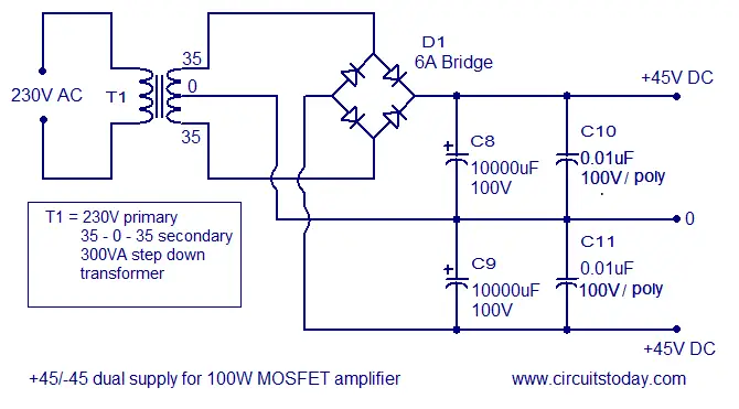
+45 / -45 dual supply for the 100W mosfet power amplifier
A basic dual power supply is used for the amplifier circuit. If 6A ampere bridge is not available, then make one using four 6A6 diodes.C10 and C11 are high frequency bypass capacitors. Filter capacitors C8 and C9 must be at least 10000uF, higher the value lesser the ripple. Optional 3A fuses can be added to the +45 and -45 lines. Transformer T1 can be a 230V primary, 35-0-35 V secondary, 300VA step down transformer.

BA5417 stereo power amplifier.

BA5417 stereo power amplifier.

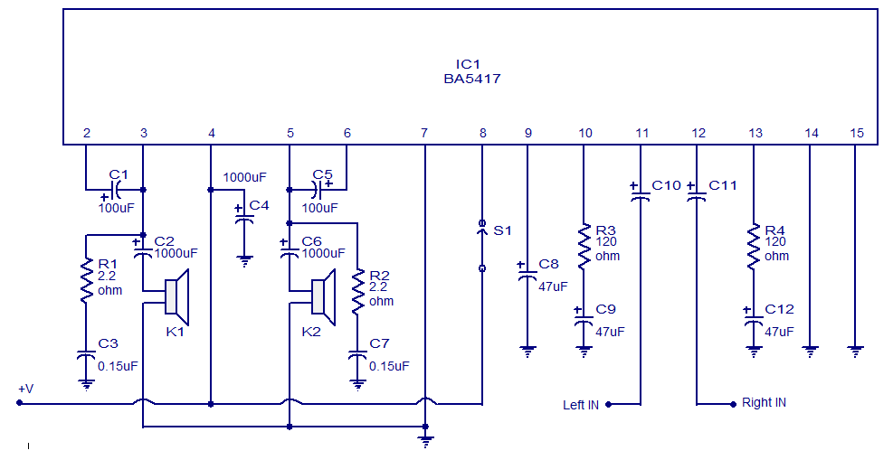
BA5417 is a stereo amplifier IC with a lot of good features like thermal shut down, standby function, soft clipping, wide operating voltage range etc. The IC can deliver 5W per channel into 4 ohm loud speakers at 12V DC supply voltage. The BA5417 has excellent sound quality and low THD (total harmonic distortion) around 0.1% at F=1kHz; Pout=0.5W.

Description.

Setup and working of this stereo power amplifier circuit is somewhat similar to the BA5406 based stereo amplifier circuit published previously. C10 and C11 are DC decoupling capacitors which block any DC level present in the input signals. C2 and C6 couples the amplifiers left and right power outputs to the corresponding loud speakers. C1 and C5 are bootstrap capacitors. Bootstrapping is a method in which a portion of the amplifiers is taken and applied to the input. The prime objective of bootstrapping is to improve the input impedance. Networks R1,C3 and R2,C7 are meant for improving the high frequency stability of the circuit. C4 is the power supply filter capacitor. S1 is the standby switch. C8 is a filter capacitor. R3 and R4 sets the gain of the left and right channels of the amplifier in conjunction with the 39K internal feedback resistors.

Circuit diagram.

stereo amplifier circuit BA5417
BA5417 stereo amplifier circuit


Notes.

  • Supply voltage range of BA5417 is from 6 to 15V DC.
  • The recommended supply voltage for this circuit is 12V DC.
  • The power supply must be well regulated and filtered.
  • BA5417 requires a heatsink.
  • The circuit can be assembled on a perf board without much degradation in performance.

Few other stereo amplifier circuits that you may like.

BA5406 stereo amplifier circuit : Simple stereo amplifier circuit that can deliver 5 watt per channel sound output into a 4 ohm speaker. Operates from 12V DC and requires very few external components. Suitable for low power car audio applications.
TDA1554 stereo amplifier circuit:  A very popular stereo amplifier design. This amplifier can output 22 watts per channel into 4 ohm loud speakers. This circuit can be also powered from 12V DC. Low distortion and noise.
2×32 watts stereo amplifier circuit : High quality stereo amplifier design using TDA2050 IC. The circuit requires a +/-18V DC dual supply. Power output is 32 watts per channel into 4 ohm speakers.
Stereo amplifier based on TDA4935 : A stereo amplifier design with a lot of great features like over load protection and thermal shut down. The power out put is 2×15 W into 4 ohm speakers. Operating voltage is 24V DC. Potentiometers for controlling the volume is also included in the circuit.
120W stereo amplifier circuit : A powerful stereo amplifier design using LM4780 audio amplifier IC from National Semiconductors. operates from a +/-35V DC dual power supply. 2×60 watt power output into 8 ohm loud speakers. The circuit has good power supply rejection and also there is a built in mute circuitry.

2N3055 Power Amplifier

2N3055 Power Amplifier
author:
Jacint Chapo

Simple and low cost. The optimal supply voltage is around 50V, but this amp work from 30 to 60V. The maximal input voltage is around 0.8 - 1V. As you can see, in this design the components have a big tolerance, so you can build it almost of the components, which you find at home. The and transistors can be any NPN type power transistor, but do not use Darlington types... The output power is around 60W.


Some comments:
- capacitor C1 regulates the low frequencies (bass), as the capacitance grows, the low frequncies are getting louder.
- capacitor C2 regulates the higher frequencies (treble), as the capacitance grows, the higher frequencies are getting quiter.
- this is a class B amplifier, this means, that a current must flow through the end transistors, even if there is no signal on the input. This current can be regulated with the 500Ω trimmer resistor. As this current incrases, the sound of the amplifier gets better, but the end transistors are more heating. But if this current decrases, the transistors are not heating so much, but the sound gets worse...


Amplifier schematic:

Jacint Chapo
14. 9. 2005.